Pin Configuration:
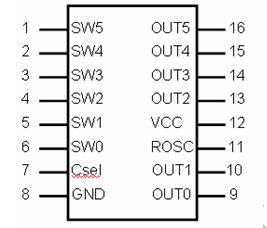
WTC6106BSI pin configuration diagram is shown in the figure below :

Definitions of Pins:
The definitions of WTC6106BSI pins are as shown in the table below:
Pin No. | Pin Name | Usage | Function Description |
1 | SW5 | | | Interface of touch key 5 (sense element 5) |
2 | SW4 | | | Interface of touch key 4 (sense element 4) |
3 | SW3 | | | Interface of touch key 3 (sense element 3) |
4 | SW2 | | | Interface of touch key 2 (sense element 2) |
5 | SW1 | | | Interface of touch key 1 (sense element 1) |
6 | SW0 | | | Interface of touch key 0 (sense element 0) |
7 | CSEL | | | Capacitor interface for adjusting the sensitivity |
8 | GND | | | Power ground |
9
| OUT0 | O | SW0 status output
|
10 | OUT1 | O | SW1 status output
|
11 | ROSC | | | Connect the 10K pull-up resistor |
12 | VCC | | | Power input |
13 | OUT2 | O | SW2 status output
|
14 | OUT3 | O | SW3 status output
|
15 | OUT4 | O | SW4 status output
|
16 | OUT5 | O | SW5 status output
|
Peripheral Circuit and Precautions:
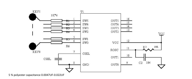
Figure 3 is the application circuit diagram of WTC6106BSI working under the 6 key mode
R1-R6 are the match resistance group. Please try to place them close to the IC

Figure 3: WTC6106BSI Application Schematic Diagram
Output Display:
When an effective touch is detected on the sensor disc, WTC6106BSI outputs the state of the corresponding sensor channel in 100ms so that the user MCU can process it, or directly drive the execution circuit work.
Take the SW0 channel for example, the relationship between the output signal and the input channel of the
sensor is shown in figure 2, and the other channels are the same.

Figure 2: Sequence diagram of WTC6106BSI key output