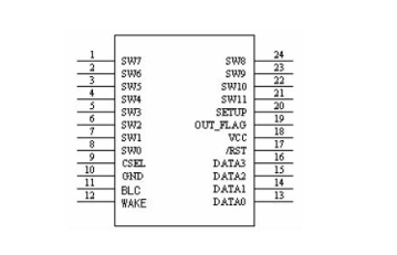
Definitions of WTC6212ML Pins:

Figure 2:
Definitions of WTC6212ML Pins:
| Pin No. | Pin Name | Usage | Function Description |
| 1 | SW7 | | | Interface of touch key 7 (sense element 7) |
| 2 | SW6 | | | Interface of touch key 7 (sense element 6) |
| 3 | SW5 | | | Interface of touch key 7 (sense element 5) |
| 4 | SW4 | | | Interface of touch key 7 (sense element 4) |
| 5 | SW3 | | | Interface of touch key 7 (sense element 3) |
| 6 | SW2 | | | Interface of touch key 7 (sense element 2) |
| 7 | SW1 | | | Interface of touch key 7 (sense element 1) |
| 8 | SW0 | | | Interface of touch key 7 (sense element 0) |
9
| CSEL | | | Capacitor interface for adjusting the sensitivity |
| 10 | GND | | | Power ground |
| 11 | BLC | | | When the backlight controls foot and the chip are awakened, the lowlevel is output, and when it is dormant, the high level is output. |
| 12 | WAKE | O | Mechanical key awakens the foot |
| 13 | DATA0 | O | BCD code output |
| 14 | DATA1 | O | BCD code output |
| 15 | DATA2 | O | BCD code output |
| 16 | DATA3 | O | BCD code output |
17
| /RST | | | Chip reset pin |
| 18 | VCC | | | positive power supply output |
| 19 | OUT_FLAG | O | Key status indicator: when there is no button pressed, it is high level, and when there is key pressed, it is low level |
| 20 | SETUP | | | Internal test foot, fixed connecting to VCC |
| 21 | SW11 | | | Interface of touch key 11 (sense element 11) |
| 22 | SW10 | | | Interface of touch key 11 (sense element 10) |
| 23 | SW9 | | | Interface of touch key 11 (sense element 9) |
| 24 | SW8 | | | Interface of touch key 11 (sense element 8) |
Output Display:
The real list of BCD output
Peripheral Circuit and Precautions:
Peripheral Circuit
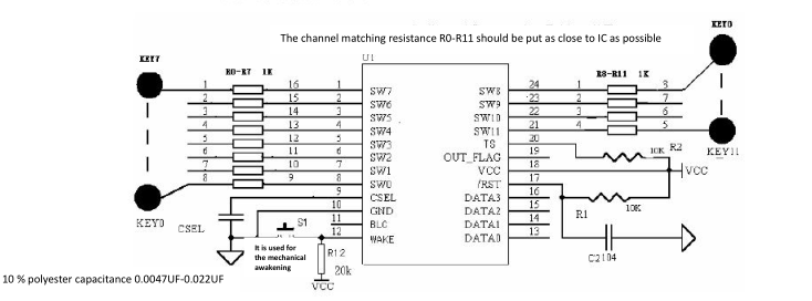
The peripheral circuit of WTC6212ML is simple and requires only a small amount of resistance. Figure 4 is the application circuit diagram of WTC6212ML working under the 12 key mode

Figure 3: WTC6212ML Application Schematic Diagram