Pin Configuration:

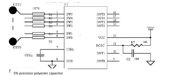
Figure 1: WTC1006BSI Pin Diagram
Definitions of Pins:
The definitions of WTC1006BSI pins are as shown in the table below:
| Pin No. | Pin Name | Usage | Function Description |
| 1 | SW5 | | | Interface of touch key 5 (sensor pad 5) |
| 2 | SW4 | | | Interface of touch key 4 (sensor pad 4) |
| 3 | SW3 | | | Interface of touch key 3 (sensor pad 3) |
| 4 | SW2 | | | Interface of touch key 2 (sensor pad 2) |
| 5 | SW1 | | | Interface of touch key 1 (sensor pad 1) |
| 6 | SW0 | | | Interface of touch key 0 (sensor pad 0) |
| 7 | CSEL | | | Capacitor interface for adjusting the sensitivity |
| 8 | GND | | | Power ground |
9
| OUT0 | O | SW0 status output. Normally it is in high impedance state, and when it is effectively touched, it will output low level, and when finger leaves it, it will return to be in high impedance state. |
| 10 | OUT1 | O | SW1 status output. Normally it is in high impedance state, and when it is effectively touched, it will output low level, and when finger leaves it, it will return to be in high impedance state. |
| 11 | ROSC | | | Connected to 10K pull-up resistor |
| 12 | VCC | | | Power input |
| 13 | OUT2 | O | SW2 status output. Normally it is in high impedance state, and when it is effectively touched, it will output low level, and when finger leaves it, it will return to be in high impedance state. |
| 14 | OUT3 | O | SW3 status output. Normally it is in high impedance state, and when it is effectively touched, it will output low level, and when finger leaves it, it will return to be in high impedance state. |
| 15 | OUT4 | O | SW4 status output. Normally it is in high impedance state, and when it is effectively touched, it will output low level, and when finger leaves it, it will return to be in high impedance state. |
| 16 | OUT5 | O | SW5 status output. Normally it is in high impedance state, and when it is effectively touched, it will output low level, and when finger leaves it, it will return to be in high impedance state. |
Output Display:
In case of no effective touch after WTC1006BSI is electrified, the output ports of all keys will be in high impedance state. When effective touch is detected on the sensor pad, the corresponding output channel of WTC1006BSI will output low level within 100ms. When the figure leaves, the output channel will be recovered to be in high impedance state. Take SW0 channel as an example, the relation between its output signals and sensor input channels are shown in Figure 3, and other channels are the same.
 Figure 2: Output Sequence Diagram of WTC1006BSI Keys
Peripheral Circuit and Precautions:
The peripheral circuit of WTC1006BSI is very simple, and only needs a few resistors and capacitors. The key component is capacitor CSEL for adjusting the sensitivity and 1K resistor for measuring the matched impedance of circuit. CSEL should use 10%-precision polyester capacitor, capacitor made of X7R material or capacitor made of NOP material. 1K resistance group can provide the best and most stable measurement effect, and CSEL and matched resistance shall be placed as close as possible to IC at PCB layout. Figure 3 is application circuit diagram of WTC1006BSI in 6-key mode:
The matched resistance R1~6 should be placed close to IC as much as possible.

Figure 3: WTC1006BSI Application Schematic Diagram