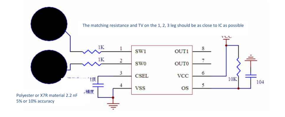
WTC6104BSI Pin Diagram:

Definitions of Pins:
The definitions of WTC02SP pins are as shown in the table below:
| Pin No. | Pin Name | Usage | Function Description |
| 1 | SW1 | | | Interface of touch key 1 (sense element 1) |
| 2 | SW0 | | | Interface of touch key 0 (sense element 0) |
| 3 | CSEL | | | Capacitor interface for adjusting the sensitivity |
| 4 | GND | | | Power ground |
| 5 | OS | | | Output mode selection The connected VCC is two keys which is the normal light touch key mode, and the connected GND OUT0 is the self-locking key output mode, and OUT1 is the PWM dimming output |
| 6 | VCC | | | Power input |
7
| OUT0 | O | SW0 status output |
| 8 | OUT0 | O | SW1 status output |
Peripheral Circuit and Precautions:
The peripheral circuit of WTC02SP is very simple, and only needs a few resistors and capacitors. The key component is capacitor CSEL for adjusting the sensitivity and IK resistance group for measuring the matched impedance of circuit. CSEL should use 10%-precision polyester capacitor, capacitor made of NOP material or capacitor made of X7R material . 1K resistance group can provide you with the best and most stable measurement effect, and CSEL and matched resistance shall be placed as close as possible to IC at PCB layout.

Figure 4: WTC02SP Application Schematic Diagram
Output Display:
When the occurrence of effective touch on the sense element is detected, WTC02SP will output the status of corresponding sense element channel within 100ms, so that it can be processed by user MCU, or directly drive the execution circuit to work. WTC02SP has two output modes. It is selected by the VCC or GND of the OS leg of IC.
1. Light touch key mode: pin OS connecting to VCC
When OS I connecting to VCC, the output mode of the general light touch key is used for the corresponding output of WTC02SP SW0 and SW1. After the effective touch is detected on the induction disc, the corresponding indicator pin outputs the low level. After he finger is left, the indicating pin restores the output high level. Taking SW0 channel as an example, the relationship between the output signal and the input channel of the sensor is shown in figure 2
The SW1 channel is the same. When OUT0 and OUT1 are electrified, the initial electrical level is the high level

Figure 2: key output timing diagram of WTC02SP OS when receiving VCC
2. Self-locking switch and PWM dimming mode: pin OS connecting to GND

Figure 3:The SW0 key outputs the sequence diagram when the WTC02SP pin OS is connected to GND