Pin Configuration:
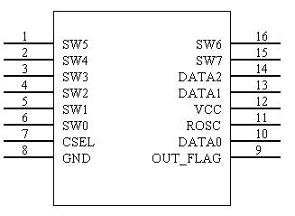
WTC6208BSI pin configuration diagram is shown in the figure 1 below :

Figure 1: WTC6208BSI Pin Diagram
Definitions of WTC62K1R Pins:
The definitions of WTC6208BSI pins are as shown in the table below:
Pin No. | Pin Name | Usage | Function Description |
1 | SW5 | | | Interface of touch key 5 (sense element 5) |
2 | SW4 | | | Interface of touch key 5 (sense element 4) |
3 | SW3 | | | Interface of touch key 5 (sense element 3) |
4 | SW2 | | | Interface of touch key 5 (sense element 2) |
5 | SW1 | | | Interface of touch key 5 (sense element 1) |
6 | SW0 | | | Interface of touch key 0 (sense element 0) interface |
7 | CSEL | | | Capacitor interface for adjusting the sensitivity |
8 | GND | | | Power ground |
9
| OUT_FLAG | O | Key state indicator: 1 indicates that the key has no effective touch; 0 indicates that there is a key pressed
|
10 | DATA0 | | | BCD code output |
11 | ROSC | | | Sensitivity adjustable capacitor interface |
12 | VCC | | | Power input |
13 | DATA1 | O | BCD code output |
14 | DATA2 | O | BCD code output |
15 | SW7 | | | Interface of touch key 7 (sense element 7)
|
16 | SW6 | | | Interface of touch key 16(sense element 6)
|
Output Display:

Figure 2: Sequence diagram of WTC6208BSI key output
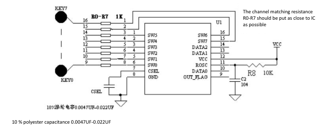
Peripheral Circuit and Precautions:

Figure 3: WTC6208BSI Application Schematic Diagram