Definitions of WTC6312BSI(W) Pins:

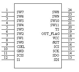
Figure 1:WTC6312BSI(W) pin configuration diagram
The definitions of WTC6312BSI(W) pins:
| Pin No. | Pin Name | Usage | Function Description |
| 1 | SW7 | | | Sense element of key 7 |
| 2 | SW6 | | | Sense element of key 6 |
| 3 | SW5 | | | Sense element of key 5 |
| 4 | SW4 | | | Sense element of key 4 |
| 5 | SW3 | | | Sense element of key 3 |
| 6 | SW2 | | | Sense element of key 2 |
| 7 | SW1 | | | Sense element of key 1 |
| 8 | SW15 | | | Sense element of key 0 |
9
| CSEL | | | Capacitor interface for adjusting the sensitivity |
| 10 | GND | | | Power ground |
| 11 | SCSS | | | When the selection foot of the work mode: connects VCC, the single key working mode is selected, and when it connects to GND, the multi-key combination (SHIFT) mode is selected. |
| 12 | S1 | | | The S1 must be connected to VCC usufully for the internal test foot |
| 13 | SDI | | | Data input line of the chip SPI interface |
| 14 | SDO | O | The data output line of the chip SPI interface |
| 15 | SCK | | | The clock input line of the chip SPI interface |
| 16 | SCS | | | The chip selection enabled line of the Chip SPI interface |
17
| /RST | | | Chip reset pin |
| 18 | VCC | | | positive power supply output |
| 19 | OUT_FLAG | O | The key state indicator: when there is key pressed, it outputs the low level signal of 50mS |
| 20 | TS | O | The TS must be connected to VCC usufully for the internal test foot |
| 21 | SW11 | | | Sense element of key 11 |
| 22 | SW10 | | | Sense element of key 10 |
| 23 | SW9 | | | Sense element of key 9 |
| 24 | SW8 | | | Sense element of key 8 |
Output Display:
Sequence diagram of BCD interface output
When the effective touch on the sense element occurred is detected, the foot of OUT_ FLAG of WTC6312BSI(W) within 150ms will output the level signal of 50ms. The customer can use this signal to realize the key awakening function, and at the same time, can externally connect a triode to drive a DC buzzer to realize the voice indication of the touch key . As shown in figure 2.

Figure 2: The signal driving buzzer of OUT_FLAG
OUT_FALG is an indication pulse that is output after the touch key is touched, but it does not indicate the touch time of the key. The key value of the touch key will kept on the finger all the time until the finger is left, and can it be continually read and judged in the program.
The SPI interface of WTC6312BSI(W)
SPI sequence diagram
The SPI time sequence diagram is shown in figure 3:

Figure 3: Sequence diagram of the SPI interface of WTC6312BSI(W)
Multi-key combination (SHIFT) mode
The peripheral circuit of the multi-key combination (SHIFT) mode and the matters needing attention
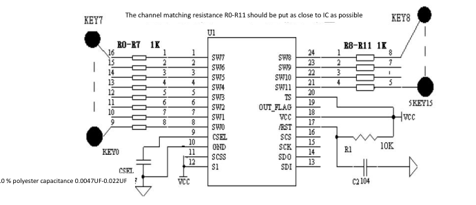
The peripheral circuit of WTC6312BSI(W) is very simple, and only needs a few resistors and capacitors. The key component is capacitor CSEL for adjusting the sensitivity and IK resistance group for measuring the matched impedance of circuit. CSEL should use 10%-precision polyester capacitor, capacitor made of NOP material paster or capacitor made of X7R material paster. 1K resistance group can provide you with the best and most stable measurement effect, and CSEL and matched resistance shall be placed as close as possible to IC at PCB layout.
Figure 5 is the application circuit diagram of WTC6312BSI(W) of WTC6312BSI(W) work under the multicity combination of 12 keys(SHIFT) mode

Figure 4: Application schematic diagram of WTC6312BSI(W) under multi-key combination (SHIFT) working mode