Definitions of WTC6312ML Pins:

Figure 1:WTC6312ML pin configuration diagram
The definitions of WTC6312ML pins:
Pin No. | Pin Name | Usage | Function Description |
1 | SW7 | | | Sense element of key 7 |
2 | SW6 | | | Sense element of key 6 |
3 | SW5 | | | Sense element of key 5 |
4 | SW4 | | | Sense element of key 4 |
5 | SW3 | | | Sense element of key 3 |
6 | SW2 | | | Sense element of key 2 |
7 | SW1 | | | Sense element of key 1 |
8 | SW0 | | | Sense element of key 0 |
9
| CSEL | | | Capacitor interface for adjusting the sensitivity |
10 | GND | | | Power ground |
11 | BLC | O | The backlight control can also be used to indicate the working state of the chip. When it is low electrical level, it indicates that the chip is in the normal working condition, and when it is high electrical level, it indicates that the chip has entered into the dormant state. At this time, the working current of the chip can be reduced to below 10uA
|
12 | WAKE | I | The external connection of the chip awakens the pin. After the chip enters the dormancy and when the foot has a change from high electrical level to low electrical level, it can immediately awaken the chip. (The interior of WAKE foot has about 30K of the upper pulling resistance).
|
13 | SDI | | | Data input line of the chip SPI interface |
14 | SDO | O | The data output line of the chip SPI interface |
15 | SCK | | | The clock input line of the chip SPI interface
|
16 | SCS | | | The chip selection enabled line of the Chip SPI interface
|
17
| /RST | | | Chip reset pin
|
18 | VCC | | | positive power supply output |
19 | OUT_FLAG | O | Key status indicator: when there is key pressed, it is the low level signal. And when all the keys are flicked, it restores to be high level
|
20 | TS | I | When the selection foot of the work mode: connects VCC, the single key working mode is selected, and when it connects to GND, the multi-key combination (SHIFT) mode is selected.
|
21 | SW8 | | | Sense element of key 8
|
22 | SW9 | | | Sense element of key 9
|
23 | SW10 | | | Sense element of key 10 |
24 | SW11 | | | Sense element of key 11 |
The SPI interface of WTC6312ML:
SPI sequence diagram
The SPI time sequence diagram is shown in figure 4:

Figure 4: Sequence diagram of the SPI interface of WTC6312ML
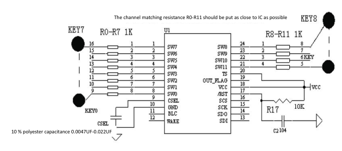
The peripheral circuit of the multi-key combination (SHIFT) mode and the matters needing attention:
The peripheral circuit of WTC6312ML is very simple, and only needs a few resistors and capacitors. The key component is capacitor CSEL for adjusting the sensitivity and IK resistance group for measuring the matched impedance of circuit. CSEL should use 10%-precision polyester capacitor, capacitor made of NOP material paster or capacitor made of X7R material paster. 1K resistance group can provide you with the best and most stable measurement effect, and CSEL and matched resistance shall be placed as close as possible to IC at PCB layout.
Figure 5 is the application circuit diagram of WTC6312ML of WTC6312ML work under the multicity combination of 12 keys(SHIFT) mode
