Definitions of WTC7514DSI(W) Pins and pin configuration diagram:

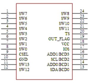
Figure 1:WTC7514DSI(W) pin configuration diagram
The table 1 is the definitions of WTC7514DSI(W) pins:
Pin No | Pin Name | Usage | Function Description |
1 | SW7 | | | Sense element of key 7 |
2 | SW6 | | | Sense element of key 6 |
3 | SW5 | | | Sense element of key 5 |
4 | SW4 | | | Sense element of key 4 |
5 | SW3 | | | Sense element of key 3 |
6 | SW2 | | | Sense element of key 2 |
7 | SW1 | | | Sense element of key 1 |
8 | SW0 | | | Sense element of key 0 |
9
| CSEL | | | Capacitor interface for adjusting the sensitivity |
10 | GND | | | Power ground |
11 | SW13 | | | Sense element of key 13 |
12 | SW12 | | | Sense element of key 12 |
13 | SDA/BCD0 | | |
The data line of the Chip IIC interface. When BCD is output, the data is 0 bit (8421 code)
|
14 | SDD0/BCD1 | O |
The address set foot of the Chip IIC interface. When BCD is output, the data is the 1 bit (8421 code) |
15 | ACL/BCD2 | | |
The clock input line of the chip IIC interface. When BCD is output, the data is 2 bit (8421 code) |
16 | ADD1/BCD3 | | |
The address set foot of the chip IIC interface. When BCD is output, the data is 3 bit (8421 code). |
17
| IOS | | |
The selected foot of output interface. When connecting GND, the IIC bus mode is making the data exchange externally. When connecting VCC, the BCD code (8421) mode to externally output key value when connecting VCC chip. |
18 | VCC | | | positive power supply output |
19 | OUT_FLAG | O |
The key state indicates that when the IOS is connected with GND, it outputs the high level pulse signal of 50mS when there is the key pressed, and when the IOS is connected with the VCC, it outputs the high level when there is the key pressed, and the low level is restored when the finger is left
|
20 | TS | | | The TS must be connected to VCC usufully for the internal test foot |
21 | SW11 | | | Sense element of key 11
|
22 | SW10 | | | Sense element of key 10 |
23 | SW9 | | | Sense element of key 9 |
24 | SW8 | | | Sense element of key 8 |
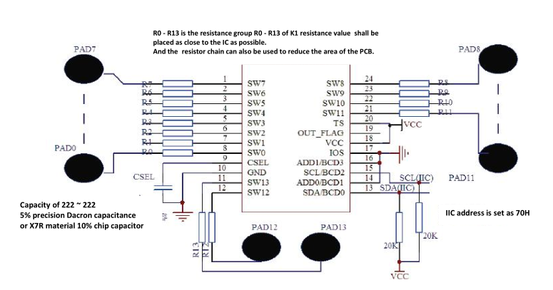
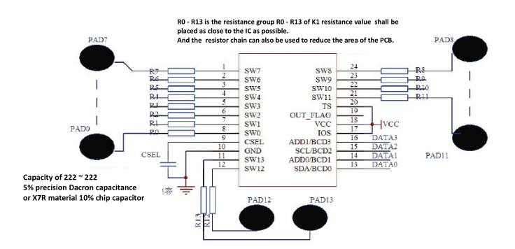
Working circuit diagram of WTC7514DSI(W)
The peripheral circuit of WTC7514DSI(W) is very simple, and only needs a few resistors and capacitors that it can work
 Figure 2: Working circuit diagram of using IIC interface of WTC7514DSI (W)

Figure 3: Working circuit diagram of using BCD code (8421) interface of WTC7514DSI (W)