Definitions of WTC6508BSI Pins And Pin Configuration Diagram:

Figure 1: WTC6508BSI pin configuration diagram
The definitions of WTC6508BSI pins are as shown in the table1 below:
Definitions of WTC62K1R Pins:
Pin No. | Pin Name | Usage | Function Description |
3 | SW5 | O | Interface of touch key 5 (sense element 5) |
4 | SW4 | O | Interface of touch key 4 (sense element 4) |
5 | SW3 | | | Interface of touch key 3 (sense element 3) |
6 | SW2 | | | Interface of touch key 2 (sense element 2) |
7 | SW1 | | | Interface of touch key 1 (sense element 1) |
8 | SW0 | | | Interface of touch key 0 (sense element 0) |
9 | CSEL | | | Capacitor interface for adjusting the sensitivity |
10 | GND | | | Power ground |
11 | SCLK | | | Clock input foot transmitted by the date |
12 | SDA | |/O | Clock output foot transmitted by the date |
17 | /RST | | | Chip reset pin |
18 | VCC | | | positive power supply output |
| BLC | O | Close to the backlight control foot |
| BUZZ | O | Buzzer control pin |
1 | SW7 | | | Interface of touch key 7 (sense element 7) |
2 | SW6 | | | Interface of touch key 6 (sense element 6) |
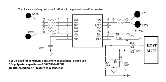
Working circuit diagram of WTC6508BSIR:

Figure 3: Working circuit diagram of WTC6508BSI
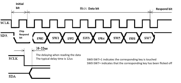
Read the touch key information:
Figure 7 is the output sequence diagram of the touch chip when the master control MCU reads the key information
