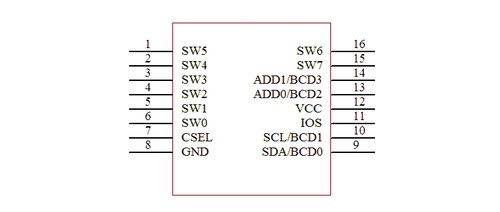
Definitions of WTC7508DSI Pins and pin configuration diagram:

Figure 1:WTC7508DSI pin configuration diagram
The table 1 is the definitions of WTC7508DSI pins:
Pin No. | Pin Name | Usage | Function Description |
1 | SW5 | | | Sense element of key 5 |
2 | SW4 | | | Sense element of key 4 |
3 | SW3 | | | Sense element of key 3 |
4 | SW2 | | | Sense element of key 2 |
5 | SW1 | | | Sense element of key 1 |
6 | SW0 | | | Sense element of key 0 |
7 | CSEL | | | Capacitor interface for adjusting the sensitivity |
8 | GND | | | Power ground |
9
| SDA/BCD0 | | | The data line of the Chip IIC interface. When BCD is o tput, the data is 1 bit (8421 code)
|
10 | SCL/BCD1 | | | The clock input line of the chip IIC interface. When BCD is output, the data is 2 bit (8421 code)
|
11 | IOS | | | The selected foot of output interface. When connecting GND, the IIC bus mode is making the data exchange externally. When connecting VCC, the BCD code (8421) mode to externally output key value when connecting VCC chip.
|
12 | VCC | | | positive power supply output |
13 | ADD0/BCD2 | | | The address set foot of the chip IIC interface. When BCD is output, the data is 3 bit (8421 code).
|
14 | ADD1/BCD3 | | | The address set foot of the chip IIC interface. When BCD is output, the data is 4 bit (8421 code).
|
15 | SW7 | | | Sense element of key 7 |
16 | SW6 | | | Sense element of key 6
|
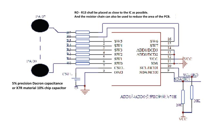
Working circuit diagram of WTC7508DSI:

Figure 2: Working circuit diagram of using IIC interface of WTC7508DSI
ADD1,ADD0 设定 IC 地址为 70H

Figure 3: Working circuit diagram of using BCD code (8421) interface of WTC7508DSI
Data when BCD code is output:
When there is no finger touch the induction disk chip, the data output by BCD3~BCD0 pin is 0(8421 code). When the effective touch on induction disk occurred is detected, in 150ms, through BCD3~BCD0 pin, WTC7508DSI outputs the BCD code of the corresponding plate channel, so that to deal with MUC when finger is left the induction disk, theBCD3~BCD0 pin recovers to be 0
The following figure is a sequence diagram of BCD data output
